Imec demonstrates 16nm pitch Ru lines with record-low resistance
A cost-effective approach to patterning the first local interconnect metal layer of A7 and beyond logic nodes.
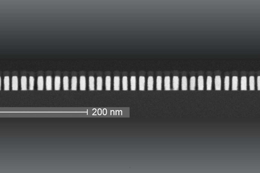
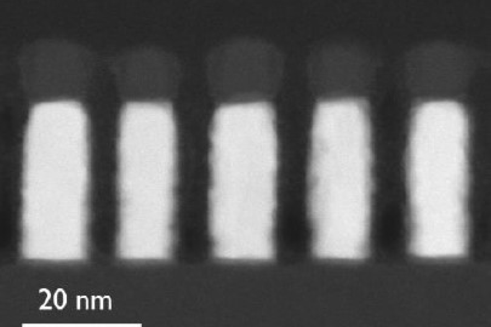
This week, at the 2025 IEEE International Interconnect Technology Conference (IITC), imec presents Ru lines at 16nm pitch with average resistance as low as 656W/µm. The 16nm pitch metal lines were fabricated using a semi-damascene integration flow optimized for cost-effective manufacturability, making it an attractive approach for fabricating the first local interconnect metal layer of the A7 and beyond technology nodes.
Ruthenium (Ru) semi-damascene has been originally proposed by imec as an attractive module approach to address the increasing resistance-capacitance (RC) delay concerns associated with Cu dual-damascene when metal pitches scale below 20nm. Semi-damascene is a two-level metallization module that starts with the direct etch of the first local interconnect metal layer (M0) and is potentially expandable to multiple layers. In 2022, imec for the first time experimentally demonstrated direct etched low-resistance Ru lines at 18nm metal pitch and expanded the integration scheme towards a two-metal-level module using fully self-aligned vias (FSAVs).
Imec now presents 16nm pitch direct etched Ru lines with a record-low average resistance of 656W/µm. 40% of the 16nm pitch Ru line structures were shown to meet the resistance target (as predicted based on thin film resistivity), corresponding to 8nm-wide local interconnects. For the 18-22nm pitch range, full-wafer yields of 90% and higher were obtained.
The presented semi-damascene integration flow relies on a modified EUV-based self-aligned double patterning (SADP) approach – referred to as spacer-is-dielectric (SID) SADP – in combination with direct etch of Ru. Three key elements from the integration flow are critical to achieving low resistance values and ensuring cost-effective manufacturability. First, the choice of cheap oxide and nitride-based materials for the hard masks, spacers and gap fill. Second, the implementation of a pattern inversion step in combination with an optimized SiO2 gap fill. And third, an improved Ru etch step during which the oxidation of the SiN hard mask was minimized to avoid line bridge defectivity.
Seongho Park, nano-interconnect program director at imec: “Now that industry is picking up Ru direct metal etch, imec is looking ahead to future generations and discusses further optimizations to its semi-damascene flow as well as new integration options. In an invited paper, imec shows advances in pillar-based FSAV approaches that are key to expanding the integration towards a two-metal-level scheme. In other papers presented at 2025 IITC, besides Ru patterning optimization, strategies to mitigate thermally induced morphology changes are investigated. Looking further ahead, imec experimentally demonstrates an epitaxially grown 25nm thin film of Ru to result in much lower resistive interconnects, approaching for the first time the bulk resistivity of Ru in the thin film regime.” At 2025 IITC, imec will be present with 20 contributions, confirming the leading role of imec and its ecosystem of partners in advancing the interconnect roadmap for the next ten years.