Positioning wafers with micrometer precision for PECVD coating

Vision-assisted robotics for handling delicate products with high accuracy.
For loading and unloading workpiece carriers containing wafers of different sizes in an automated process prior to PECVD coating, acp systems has developed a robotic solution aided by image processing for a leading manufacturer of space solar technology. It ensures that the specified positioning accuracy of +/- 0.1 mm in the nests of the workpiece carriers is met and that both the manufacturing tolerances of the carriers and their shrinkage caused by cooling during loading are compensated for.
Azur Space Solar Power GmbH, which is based in Heilbronn, is one of the world’s leading companies that develops and produces highly efficient multi-junction solar cells for space and terrestrial concentrator systems (CPV). All solar cells are based on the latest triple and quadruple junction technology, in which the layers are built up on a germanium substrate.
Automating the challenging loading and unloading process
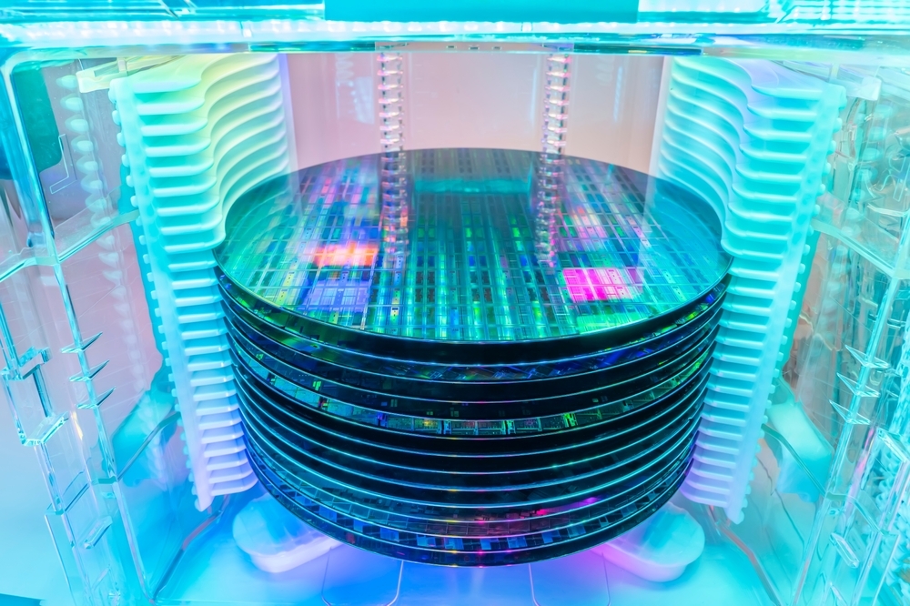
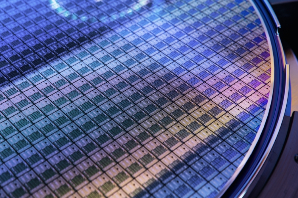
During the production process, the 4-, 6- and 8- inch (100, 150 and 200 mm) diameter wafers undergo a PECVD process (plasma-enhanced chemical vapor deposition) in systems from Singulus Technologies AG. The solar cells are supplied in cassettes, removed from them and placed in the nests of special carbon fiber workpiece carriers, which are just a few hundred micrometers larger. Depending on the cell size, the 1000 x 600 mm carriers can hold four, nine or 16 wafers. To avoid collisions, a positioning accuracy of +/- 0.1 mm must be reliably met when loading the workpiece carriers. After being coated on one or both sides, the solar cells must then be placed back into cassettes.
Azur Space wanted to automate this previously time-consuming and cost-intensive manual process using suction pipettes. The position of the solar wafers with flats in the cassettes can deviate by +/- 5 degrees and +/- 3 mm and the gripping points are precisely defined, making this quite a challenge. In addition, the production-related tolerances of the carriers have to be compensated for, as must the shrinkage caused
by cooling. This is due to the falling temperature of the workpiece carriers, which come out of the coating process at up to 350 °C and cool down during unloading and loading.
Positioning accuracy ensured with illuminated alignment table and image processing
To realize this task, automation specialist acp systems AG developed an intelligent, vision-assisted handling solution with an industrial robot. Due to the limited space available, this was mounted on the ceiling of the loading area of the coating system and has a reach of 1,000 millimeters. The Scara robot is equipped with a special flat vacuum gripper system that can be quickly exchanged to handle wafers of different sizes.
The robot takes out the wafer from the cassette and places it on a backlit alignment table. A camera system with a 12-megapixel camera is located above the table at a working distance of 680 mm. It detects the exact position of the wafer and sends this information to the Cognex Vision Pro software. Based on this, the software calculates the position and angle of compensation required to insert the wafer into the carrier nest and transmits the data to the robot controller. Any distortions in the camera system were compensated for during commissioning by calibrating it with a checker plate.
In order to overcome the manufacturing tolerances of the carriers and the shrinkage caused by cooling, each workpiece carrier is first centered by pulling it against a stop and indexing it. This allows the coordinate zero point of all carriers in the handling system to be reproducibly defined. Furthermore, to compensate for manufacturing tolerances, all carriers were accurately measured beforehand in their cold, new state and each was given a data matrix code for identification. This code is used to store relevant data in the controller so that the position tolerances of the carrier nests can be calculated and compensated for.
To compensate for the thermal shrinkage caused by the workpiece carriers cooling down, a fiducial mark was first placed in the corner of each carrier opposite the coordinate zero point, and this was also accurately measured precisely when cold. A second camera system is located above this, enabling the offset of the fiducial mark compared to the cold state to be determined. The software uses this information to calculate the compensation needed to set down the wafer accurately in position. This process is repeated for each wafer to be inserted.
Flipping station for turning the wafers
acp systems also integrated a flipping station for turning the solar cells so that they can be coated on both sides. This receives the corresponding wafers one by one from the robot and grips them at defined points with vacuum suction dots. After the wafer has been rotated by 180 degrees, the robot gripper picks it up again and transfers it to the alignment table.
Integrated quality control
Before the coated solar cells are placed back into the cassettes, a final quality check is carried out by the camera system on the alignment table. This checks whether the edges of the wafers are free of damage.
The vision-assisted robotic solution described above ensures that the extremely delicate solar wafers are handled with high precision and care. This is demonstrated above all by the fact that there have been no handling-related wafer breakages since commissioning. Overall, replacing manual handling with a fully automated system has resulted in significantly improved productivity and efficiency.